APPLIED MATERIALS INTRODUCES MATERIALS ENGINEERING SOLUTIONS FOR DRAM SCALING
Applied Materials, Inc. today announced materials engineering solutions that give its memory customers three new ways to further scale DRAM and accelerate improvements in chip performance, power, area, cost and time to market (PPACt).
- New Draco hard mask material co-optimized with Sym3® Y etcher to accelerate DRAM capacitor scaling
- DRAM makers adopting Black Diamond®, the low-k dielectric material pioneered by Applied Materials to overcome interconnect scaling challenges in logic
- High-k metal gate transistors now being introduced in advanced DRAM designs to boost performance and reduce power while shrinking the periphery logic to improve area and cost
The digital transformation of the global economy is generating record demand for DRAM. The Internet of Things is creating hundreds of billions of new computing devices at the edge which are driving an exponential increase in data transmitted to the cloud for processing. The industry urgently needs breakthroughs that can allow DRAM to scale to reduce area and cost while also operating at higher speeds and using less power.
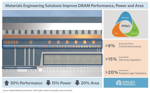
Applied Materials is working with DRAM customers to commercialize three materials engineering solutions that create new ways to shrink as well as improve performance and power. The solutions target three areas of DRAM chips: storage capacitors, interconnect wiring and logic transistors. They are now ramping into high volume and are expected to significantly increase Applied’s DRAM revenue over the next several years.
Introducing Draco Hard Mask for Capacitor Scaling
Since over 55 percent of a DRAM chip’s die area is occupied by the memory arrays, increasing the density of these cells is the biggest lever for reducing cost per bit. Data is stored as charges in cylindrical, vertically arranged capacitors that need as much surface area as possible to hold adequate numbers of electrons. As DRAM makers narrow the capacitors, they also elongate them to maximize surface area.
A new technology challenge to DRAM scaling has emerged: the etching of the deep capacitor holes threatens to exceed the limits of the “hard mask” material that acts as a stencil to determine where each cylinder is placed. If the hard mask is etched through, the pattern is ruined. Taller hard masks are not viable because as the combined depth of the hard masks and capacitor holes exceeds certain limits, etch byproducts remain and cause bending, twisting and uneven depths.
The solution is Draco, a new hard mask material that has been co-optimized to work with Applied’s Sym3® Y etch system in a process monitored by Applied’s PROVision® eBeam metrology and inspection system that can take nearly half a million measurements per hour. The Draco hard mask increases etch selectivity by more than 30 percent which enables a shorter mask.
Draco hard mask and Sym3 Y co-optimization includes advanced RF pulsing which synchronizes etching with byproduct removal to enable patterning holes that are perfectly cylindrical, straight and uniform. The PROVision eBeam system gives customers massive, immediate actionable data on hard mask critical dimension uniformity which is the key to capacitor uniformity. Applied’s solution provides customers with a 50-percent improvement in local critical dimension uniformity and reduces bridge defects by 100X, thus increasing yields.
“The best way to quickly solve materials engineering challenges with our customers is to co-optimize adjacent steps and use massive measurements and AI to optimize process variables,” said Dr. Raman Achutharaman, group vice president, Semiconductor Products Group at Applied Materials.
Bringing Black Diamond® Low-k Dielectric to the DRAM Market
A second key lever of DRAM scaling is reducing the die area needed by the interconnect wiring that routes signals to and from the memory arrays. Each of the metal lines is surrounded by an insulating dielectric material to prevent interference between data signals. For the past 25 years, DRAM makers have used one of two silicon oxides – silane and tetraethoxysilane (TEOS) – as the dielectric material.
Continual thinning of the dielectric layers has reduced DRAM die sizes but created a new technology challenge: the dielectrics are now too thin to prevent capacitive coupling in the metal lines whereby signals interfere with one another causing higher power consumption, slower performance, increased heat and reliability risks.
The solution is Black Diamond®, a low-k dielectric material first used in advanced logic. With DRAM designs now experiencing similar scaling challenges, Applied is adapting Black Diamond to the DRAM market and making it available on the highly productive Producer® GT platform. Black Diamond for DRAM enables smaller, more compact interconnect wires that can move signals through the chips at multi-gigahertz speeds without interference and at lower power consumption.
High-k Metal Gate Transistors Bring PPAC Improvements to DRAM
A third key lever of DRAM scaling is improving the performance, power, area and cost of the transistors used in the periphery logic of the chip to help drive the input-output (I/O) operations needed in high-performance DRAM like those based on the new DDR5 specification.
Until today, DRAM used transistors based on polysilicon-oxide which were phased out in foundry-logic by the 28-nanometer node because extreme thinning of the gate dielectric allowed electrons to leak, thereby wasting power and limiting performance. Logic makers adopted high-k metal gate (HKMG) transistors, replacing the polysilicon with a metal gate and the dielectric with hafnium oxide, a material that improves gate capacitance, leakage and performance. Now memory makers are designing HKMG transistors into advanced DRAM designs to improve performance, power, area and cost. In DRAM as in logic, HKMG will increasingly replace polysilicon transistors over time.
This technology inflection in DRAM creates growth opportunities for Applied Materials. The more complex and delicate HKMG materials stack is challenging to manufacture, and in-vacuum processing of adjacent steps using Applied’s Endura® Avenir RFPVD system has become the industry’s preferred solution. HKMG transistors also benefit from Applied’s epitaxial deposition technologies such as Centura® RP Epi along with film treatments including RadOx RTP, Radiance® RTP and DPN which are used to fine-tune the transistor characteristics for optimum performance.
“Draco hard mask and Black Diamond low-k dielectric are being adopted by leading DRAM customers, and the first HKMG DRAMs are now being introduced,” added Dr. Achutharaman. “Applied Materials projects billions of dollars in revenue growth as these DRAM inflections play out over the next several years.”
Additional information about the growth outlook for these technologies is being provided at Applied’s 2021 Memory Master Class being held later today. For more information, please visit the investor page of our website at https://ir.appliedmaterials.com.
Forward-Looking Statements
This release contains forward-looking statements, including those regarding anticipated growth and trends in our revenues, businesses and markets, industry outlooks and demand drivers, technology transitions, new products and technologies, and other statements that are not historical facts.
These statements and their underlying assumptions are subject to risks and uncertainties and are not guarantees of future performance. Factors that could cause actual results to differ materially from those expressed or implied by such statements are described in our SEC filings, including our recent Forms 10-Q and 8-K. All forward-looking statements are based on management’s current estimates, projections and assumptions, and we assume no obligation to update them.
www.appliedmaterials.com